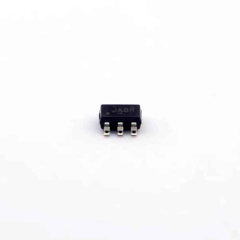
This comprehensive guide explores common issues faced by users of the TS5A3159DBVR analog switch IC, highlighting troubleshooting techniques and solutions to ensure consistent performance. Whether you're an engineer or a hobbyist, this article will help you diagnose and fix problems, keeping your designs functioning efficiently.
TS5A3159DBVR, analog switch, troubleshooting, solutions, IC performance, common issues, circuit design, troubleshooting guide, signal routing, signal switching
Understanding TS5A3159DBVR and Identifying Common Issues
The TS5A3159DBVR is a low-voltage, bidirectional, analog switch from Texas Instruments, designed for high-performance signal routing in a wide range of applications, including audio processing, video switching, and data transmission. While it is known for its reliability and versatility, engineers and designers sometimes encounter issues that affect its performance.
In this article, we’ll walk through common troubleshooting scenarios and provide effective solutions to ensure that your TS5A3159DBVR operates as expected in your designs. Let's begin by examining some of the typical challenges that users may face when integrating this IC into their circuits.
1. Incorrect Voltage Levels
The TS5A3159DBVR is a low-voltage device that operates in the range of 1.65V to 5.5V. One of the most common issues users encounter is incorrect voltage levels that cause improper switching behavior or even damage to the IC.
Symptoms:
Unresponsive switches
Inconsistent signal paths
Circuit malfunction
Solution:
Ensure that the supply voltage to the IC is within the specified range. If the input voltage is higher than the maximum rated voltage (5.5V), it may cause irreversible damage to the device. Likewise, operating below the minimum threshold of 1.65V can lead to improper switching.
Tips for Proper Voltage Handling:
Always check the supply voltages with a multimeter before powering up the circuit.
Use a voltage regulator or level shifter to ensure the voltage remains within safe limits.
If you are using a battery-powered design, check the battery voltage under load conditions, as it may fluctuate and fall outside the operating range of the IC.
2. Floating Control Pins
One of the most common issues when working with analog switches like theTS5A3159DBVR is improperly managed control pins. These control pins determine whether the switch is open or closed, and if left floating, they may cause erratic switching behavior.
Symptoms:
Random switching behavior
Unstable or fluctuating signals
Solution:
Control pins should never be left floating. Ensure that they are connected to a defined logic level, either high or low, depending on the desired switch behavior. This is crucial for maintaining reliable performance.
Best Practices for Control Pins:
Use pull-up or pull-down resistors to set the default state of the control pins.
If the control signal is coming from a microcontroller or FPGA, ensure that the GPIO pin is configured as an output with a defined voltage level.
For multi-channel designs, ensure that each control pin is managed independently to prevent cross-talk or unwanted switching.
3. Grounding Issues
Poor grounding is another common cause of instability in analog circuits, including those involving the TS5A3159DBVR. Insufficient or improper grounding can result in noise, signal degradation, or even erratic switching behavior.
Symptoms:
Signal noise
Intermittent switching
Unexpected voltage drops
Solution:
Proper grounding is essential for the reliable operation of the TS5A3159DBVR. Ground loops or shared ground paths with noisy components can introduce unwanted signals that affect the switch’s performance.
Solutions for Grounding:
Use a dedicated ground plane for the analog section of your circuit to minimize noise interference.
Ensure that the ground connection is solid, with low resistance, and avoid long ground traces.
If possible, use a star grounding configuration to prevent high-current paths from interfering with the analog signals.
4. Signal Integrity Problems
The TS5A3159DBVR is designed to switch analog signals, and poor signal integrity can lead to issues such as signal distortion, noise, and reduced performance. This can be particularly problematic in high-frequency applications or circuits with large signal swings.
Symptoms:
Distorted or degraded signals
Increased noise levels
Reduced signal fidelity
Solution:
Signal integrity issues are often a result of improper PCB layout, excessive capacitance, or long signal traces. These issues can become more apparent in high-speed or high-frequency circuits.
Tips to Maintain Signal Integrity:
Keep signal paths as short and direct as possible to reduce parasitic inductance and capacitance.
Use proper decoupling capacitors (typically 0.1µF and 10µF) close to the power supply pins to filter high-frequency noise.
If you are switching high-frequency signals, use controlled impedance traces to match the impedance of the source and load.
For high-speed designs, ensure that the PCB layout minimizes crosstalk between adjacent signal traces.
5. Overheating and Power Dissipation
Although the TS5A3159DBVR is an efficient device, it can still be susceptible to overheating under certain conditions. Excessive power dissipation may occur if the IC is used in high-current applications, or if the ambient temperature exceeds the recommended operating range.
Symptoms:
Overheating of the IC
Decreased performance
Potential damage to the IC
Solution:
The TS5A3159DBVR is designed for low-power applications, but it’s important to consider thermal management in your design.
Thermal Management Solutions:
Check the power consumption of your application and ensure it does not exceed the IC's thermal limits.
Use heat sinks or thermal vias to dissipate heat away from the device.
If possible, reduce the load current or use current-limiting resistors to prevent excessive heat generation.
Ensure good ventilation around the IC to allow heat to dissipate efficiently.
Advanced Troubleshooting Techniques and Solutions for TS5A3159DBVR
In the previous section, we covered some of the most common issues that users face when working with the TS5A3159DBVR, along with their corresponding solutions. In this section, we’ll dive deeper into more advanced troubleshooting techniques, providing insights into how you can tackle complex problems to ensure the continued success of your design.
6. Unstable Output When Switching
Occasionally, users report unstable or inconsistent output when the TS5A3159DBVR switches between different signal paths. This could be due to improper timing, insufficient drive strength, or loading effects on the switch.
Symptoms:
Glitches or spikes in the output signal when switching
Output signal not matching the input signal
Unstable signal paths during transitions
Solution:
When switching between channels, ensure that the control signals are properly synchronized and meet the timing requirements specified in the datasheet. Additionally, if the load connected to the output is too heavy, it can cause the signal to degrade or become unstable.
Best Practices:
Ensure that the switching time (t(on) and t(off)) is within the acceptable range for your application. If necessary, use a buffer or amplifier to drive heavier loads.
Minimize the load capacitance on the output of the TS5A3159DBVR by using low-capacitance components and avoiding long traces.
Use a logic analyzer or oscilloscope to monitor the signal transitions and verify that the timing and control signals align properly.
7. Crosstalk Between Channels
In designs with multiple switches, crosstalk between adjacent channels can cause interference and signal degradation. This is particularly critical in high-precision applications, such as audio or RF signal routing.
Symptoms:
Unwanted signals appear on channels that are not actively switched
Interference or noise between adjacent signal paths
Solution:
Crosstalk can occur when signal paths are too close to one another or when switching characteristics lead to coupling between channels. To minimize this, ensure that the PCB layout is optimized and that traces are spaced adequately.
Mitigating Crosstalk:
Increase the physical separation between signal traces, particularly between adjacent channels.
Use ground traces or planes between signal channels to isolate them and reduce coupling.
Ensure proper termination of unused channels to prevent floating and reduce the possibility of crosstalk.
8. Faulty or Noisy Power Supply
A noisy or unstable power supply can adversely affect the performance of the TS5A3159DBVR. Power supply noise can introduce artifacts, reduce signal integrity, or even cause the switch to malfunction.
Symptoms:
Unstable operation of the switch
Increased noise or distortion in the output signal
Inconsistent switching behavior
Solution:
Make sure that the power supply is stable and provides clean power to the IC. Using a low-noise power supply or adding decoupling capacitors can mitigate these issues.
Solutions for Power Supply Noise:
Use low-noise regulators to provide clean power to the TS5A3159DBVR.
Add decoupling capacitors (e.g., 0.1µF or 10µF) close to the power pins to filter high-frequency noise.
If using a shared power supply, ensure that the IC is adequately decoupled from other noisy components in the system.
9. Compatibility Issues with Other ICs
In some cases, the TS5A3159DBVR may not function properly when used in conjunction with other ICs, especially when there are voltage level mismatches or conflicts in signal routing.
Symptoms:
Unexpected behavior when interfacing with other ICs
Input/output conflicts or incorrect voltage levels
Solution:
Ensure that all ICs in the signal path are compatible in terms of voltage levels and logic levels. This can be especially critical in mixed-signal designs, where voltage mismatches may occur.
Best Practices:
Check the voltage level requirements of all connected ICs and use level shifters if necessary.
Ensure that all input signals are within the specified input voltage range of the TS5A3159DBVR.
When interfacing with other analog devices, consider using buffer amplifiers to ensure proper signal integrity and voltage matching.
By following the troubleshooting tips and best practices outlined in this article, you can ensure that the TS5A3159DBVR performs optimally in your application. Whether you're working on an audio switch, video router, or data switching circuit, understanding these potential pitfalls and solutions will help you maintain the integrity of your design and achieve the best performance possible from this versatile analog switch IC.
If you're looking for models of commonly used electronic components or more information about TS5A3159DBVR datasheets, compile all your procurement and CAD information in one place.
( Partnering with an electronic component supplier ) sets your team up for success, ensuring that the design, production and procurement processes are streamlined and error-free. ( Contact us ) for free today.

